 |
London, UK (SPX) Dec 02, 2010 A European consortium comprising NPL, ST Microelectronics, the University of Edinburgh, and TU Delft has been involved in the development and application of the Megaframe Imager - an ultrafast camera capable of recording images at the incredible rate of one million frames Since the introduction of solid-state optical sensors, like those found in digital cameras, the main trend has been towards increasing the resolution (i.e. number of pixels) while miniaturising the chip. However, the other factor is the number of frames the chip is capable of recording in a given time. Until recently, fast cameras (i.e. those capturing more than the 24 frames per second required for 'normal' video) were only used in niche markets in science and entertainment. Now that higher-than-video speeds are achievable, a whole new range of previously unthinkable applications have emerged - such as: cellular / sub-cellular imaging; neural imaging; biochemical sensors; DNA / protein microarray scanning; automotive collision studies; and high-sensitivity astronomical observations. The Megaframe Imager uses an extremely sensitive single photon avalanche diode (SPAD) device, and bespoke on-chip intelligence and has shown for the first time that it could potentially be a powerful technology in biosensing. Reporting in the Optical Society of America's new journal Biomedical Optics Express the research team have demonstrated detection of viral DNA binding events using fluoresence lifetime imaging at the very low target concentrations relevant in biosensing applications with acquisition times of less than 30 seconds. DNA microarrays are important tools for biomolecular detection. Widely used for gene expression profiling, disease screening, mutation and forensic analysis, they also hold much promise for the future development of personalised drugs and point of care testing devices. Read the paper in Biomedical Optics Express: Fluorescence lifetime biosensing with DNA microarrays and a CMOS-SPAD imager
Share This Article With Planet Earth
Related Links ST Microelectronics Computer Chip Architecture, Technology and Manufacture Nano Technology News From SpaceMart.com
 Manufacturing Made To Measure Atomic-Scale Electrodes
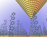
Kiel, Germany (SPX) Dec 01, 2010 Thanks to collaborative work between scientists in Donostia-San Sebastian and the University of Kiel (Germany) it has been shown that it is possible to determine and control the number of atoms in contact between a molecule and a metal electrode of copper, at the same time as the electric current passing through the union being recorded. These results were published in the Nature Nanotechnology ... read more |
|
| The content herein, unless otherwise known to be public domain, are Copyright 1995-2010 - SpaceDaily. AFP and UPI Wire Stories are copyright Agence France-Presse and United Press International. ESA Portal Reports are copyright European Space Agency. All NASA sourced material is public domain. Additional copyrights may apply in whole or part to other bona fide parties. Advertising does not imply endorsement,agreement or approval of any opinions, statements or information provided by SpaceDaily on any Web page published or hosted by SpaceDaily. Privacy Statement |