 |
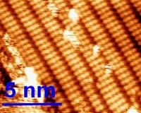
Raleigh NC (SPX) Oct 13, 2010 An approach pioneered by researchers at North Carolina State University gives scientists new insight into the way silicon bonds with other materials at the atomic level. This technique could lead to improved understanding of and control over bond formation at the atomic level, and opportunities for the creation of new devices and more efficient microchips. Manufacturers build silicon-based devices from layers of different materials. Bonds - the chemical interaction between adjacent atoms - are what give materials their distinctive characteristics. "Essentially, a bond is the glue that holds two atoms together, and it is this glue that determines material properties, like hardness and transparency," says Dr. Kenan Gundogdu, assistant professor of physics at NC State and co-author of the research. "Bonds are formed as materials come together. We have influenced the assembly process of silicon crystals by applying strain during bond formation. Manufacturers know that strain makes a difference in how bonds form, but up to now there hasn't been much understanding of how this works on the atomic level." Gundogdu, along with Dr. David Aspnes, Distinguished University Professor of Physics, and doctoral candidate Bilal Gokce, used optical spectroscopy along with a method of analysis pioneered by Aspnes and former graduate student Dr. Eric Adles that allowed them to examine what was happening on the atomic scale when strain was applied to a silicon crystal. "Strain has been used to affect overall chemistry for a long time," Aspnes says. "However, no one has previously observed differences in chemical behavior of individual bonds as a result of applying strain in one direction. Now that we can see what is actually happening, we'll gain a much better understanding of its impact on the atomic scale, and ideally be able to put it to use." According to Gundogdu, "Application of even small amount of strain in one direction increases the chemical reactivity of bonds in certain direction, which in turn causes structural changes. Up to now, strain has been applied when devices are made. But by looking at the effect on the individual atomic bonds we now know that we can influence chemical reactions in a particular direction, which in principle allows us to be more selective in the manufacturing process." "While we are able to exert some directional control over reaction rates, there remains much that we still don't understand," Aspnes adds. "Continuing research will allow us to identify the relevant hidden variables, and silicon-based devices may become more efficient as a result."
Share This Article With Planet Earth
Related Links North Carolina State University Space Technology News - Applications and Research
 Polymer Behaviors Below The 1 Nanometer Level
Kyoto, Japan (SPX) Oct 13, 2010 Knowing how to build nanosized assemblies of polymers (long molecular chains) holds the key to improving a broad range of industrial processes, from the production of nanofibers, filters, and new materials to the manufacture of low-energy, nanoscale circuits and devices. A recent paper in Nature Communications sheds light on key behaviors of polymers in specially engineered confined spaces ... read more |
|
| The content herein, unless otherwise known to be public domain, are Copyright 1995-2010 - SpaceDaily. AFP and UPI Wire Stories are copyright Agence France-Presse and United Press International. ESA Portal Reports are copyright European Space Agency. All NASA sourced material is public domain. Additional copyrights may apply in whole or part to other bona fide parties. Advertising does not imply endorsement,agreement or approval of any opinions, statements or information provided by SpaceDaily on any Web page published or hosted by SpaceDaily. Privacy Statement |